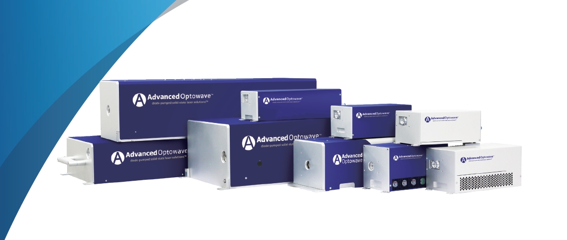


Our Products
Products We Carry
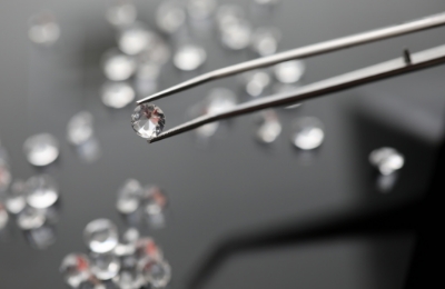
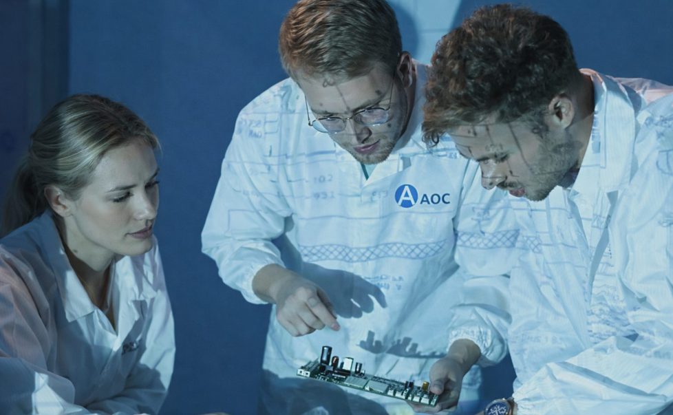
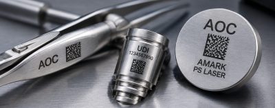
Advanced Optowave Corporation products strongly enhance our customer’s capabilities and productivity in consumer electronics, biomedical applications, semiconductor and other areas. As of today, there are more than 55,000 laser sources and laser systems installed worldwide from our innovative laser technologies. Laser for Better Life is the company mission of Advanced Optowave.


ABOUT US
Who We Are
Established in 2007, Advanced Optowave is a highly respected global supplier of diode-pumped solid-state laser solutions and laser systems. We pioneer laser technology advancements, delivering tailored solutions for various industries and research fields. Our commitment extends to providing exceptional local service and support, ensuring seamless product integration and optimal performance for our customers.
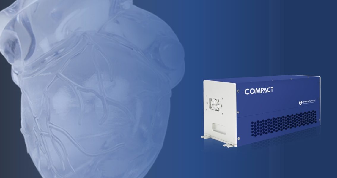
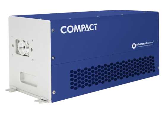
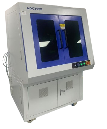
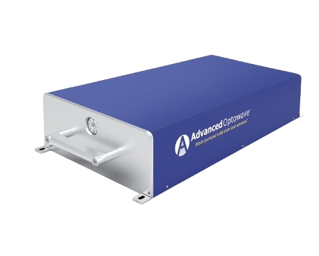
Advanced Optowave’s laser product portfolio encompasses a diverse range of pulsed lasers, including DPSS QS-ns, ultrafast, and MOPA-ns lasers, spanning wavelengths from IR to DUV and pulse widths from nanosecond to femtosecond. By leveraging innovative laser technologies and robust process development capabilities, Advanced Optowave delivers comprehensive laser application solutions to customers around the globe. With superior optical design, vision systems, motion control systems, and proprietary software, we’ve grown to be a valuable partner to Fortune 500 companies as well as small to medium sized businesses by providing cutting-edge laser solutions.
Testimonials
What Our Customers Say About Us
“We achieved higher throughput and better cosmetic quality for small electronic components with minimal thermal impact.”

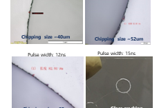
“We achieved smooth, crack-free cutting on thin glass substrates. The laser process significantly improved edge quality.”

“The laser allowed us to machine complex micro-features with excellent dimensional accuracy and minimal heat-affected zones.”
“For wafer-level micro-processing, beam quality and repeatability are essential. The system delivered reliable performance during continuous operation.”
“The laser stability and pulse-to-pulse consistency are critical for medical components. Advanced Optowave met our strict quality and validation requirements.”

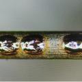
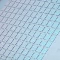
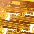
“Advanced Optowave’s nanosecond UV laser delivered excellent edge quality and minimal thermal impact on our PCB and FPC cutting processes. The laser stability and consistency significantly improved our production yield.”

50,000+
laser sources installed worldwide
18 years
in business
5,000+
laser systems installed worldwide

Events
The Latest from Advanced Optowave
Our News
The Latest from Advanced Optowave
GET IN TOUCH
Looking For Solid-State Laser Solutions?
Reach out to our experienced team today!