AOC’s strategic emphasis lies in laser and laser application R&D, global sales and marketing endeavors, and the provision of localized customer service and support.
AOC laser product portfolio consists of a broad spectrum of pulsed lasers, including DPSS QS-ns lasers, ultrafast lasers, and MOPA-ns lasers, covering different wavelengths from IR to DUV, and different pulse widths from nanosecond, picosecond to femtosecond. Combining the innovative laser technologies with laser process development capability, AOC can offer complete laser application solutions. With advanced optical design, vision system, motion control system and self-developed software, AOC is now supplying laser micro-processing systems.
AOC products strongly enhance our customer’s capabilities and productivity in consumer electronics, biomedical applications, semiconductor, and other areas. As of today, there are tens thousands laser source and micro-processing system in use in these application fields.
Unlike other frequently used metals in the industry such as stainless steel, nickel, aluminum, copper possesses unique physical properties that offer significant benefits to various applications. However, these unique properties also necessitate the exploration and development of new laser technologies for copper’s additive manufacturing (3D printing) such as green (515-532nm) laser and blue laser diode (BLD. 450nm)) because of much higher optical absorption in the range of blue (65%) – visible (55%) range of than IR (1030-1064nm) range (~5%). Thus, green laser and BLD has been gradually replaced IR laser in copper 3D printing. Currently, CW laser power bead fusion (L-PBF) is major method for 3D printing of copper.
To reach the melting temperature of 1083°C for copper, a higher laser power, up to thousands of watts, is required due to copper’s high thermal conductivity of 384 W/m·K. However, using pulsed lasers can melt metals at lower laser power because of their high peak power. The key challenge is maintaining the molten pool long enough to achieve bulk properties. Additionally, utilizing pulsed green laser technology can achieve high-precision 3D printing of copper components. This advanced manufacturing process offers superior control and accuracy, making it ideal for applications requiring intricate copper structures.
For this purpose, AOC has investigated for the first time the feasibility of 3D printing copper using long pulse nanosecond (ns) lasers. Preliminary results showed positive feasibility, although the achieved material density of 93% was slightly lower than the industry standard of over 98%. If successful, this approach could open important applications for ns-GR lasers.
It has been approved that a long-pulse nanosecond laser with high frequency demonstrates advantages in low-temperature heat treatment processes such as oxidation, annealing, sintering, and intermixing due to its high absorption by copper, high peak power, and cost-effectiveness. In this process, AOC’s specially designed long-pulse ns-532nm laser, operating at frequencies greater than 100 kHz, is utilized as shown in Figure 1.
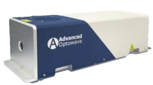
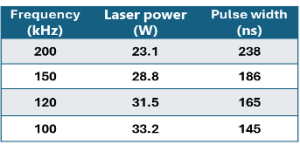
Fig.1 AOC long pulse width nanosecond 532nm laser
Commercial micro-size (30um in dia.) copper powders (Purity of 98%) were utilized. Figure 2 showcases the SEM image of the particles and their size distribution.
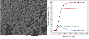
Fig. 2 Copper power particles size and distribution
The energy injection process by a pulsed laser can be viewed as a composite process of transient heating and residual heat accumulation induced by single pulses (see Figure 3). Initially, a single laser pulse injects energy into the material per unit area within the pulse duration, generating transient high temperatures. The transient temperature depends on the peak power density of the pulse.Once the laser spot area on the material surface is determined, the temperature increases with the peak power.
When a single pulse ends, the transient temperature drops, and the rate of this decrease depends on the thermal conductivity of the material. Therefore, if the next pulse is triggered while residual heat is still present, the initial temperature at this time will be higher than the initial temperature of the previous pulse. This cycle of residual heat accumulation will gradually raise the overall temperature of the material, maintaining the presence of the molten pool.
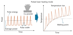
Figure 3. Schematic diagram of pulse laser heating process
The purpose of this approach is to investigate feasibility of long pulsed ns-532nm laser 3D printing of copper for industry application. To achieve pulse laser melting of metal particles, three conditions must be met: (i) Appropriate laser energy to ensure the energy density is below the material removal threshold; (ii) A pulse width as long as possible (>100 ns) to meet the peak power requirement for particle melting; (iii) A pulse repetition frequency as high as possible to ensure the time interval between pulses is close to the metal’s thermal relaxation time (on the order of microseconds). Based on the mechanism of pulse laser-induced metal powder melting, this study explores the use of a high repetition rate (up to 300 kHz), long pulse width (up to 250 ns), 532 nm wavelength laser to achieve high-density 3D printing of copper.
The study investigates the effects of laser processing parameters such as peak power and spatial two-dimensional overlap rate on the 3D printing formation of pure copper powder.
Figure 4 showcases 3D-printed copper objects with three different structures. The printed cylindrical solid copper is used for testing material density, while the printed tube and turbine blades are used for testing printing resolution.
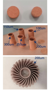
Figure 4. Printed copper cylinders, tubes and turbo blades using AOC long pulse ns-532nm laser
The wall thickness of the printed tube varies as follows: 300 µm, 250 µm, 200 µm, 150 µm, and 100 µm. The wall thickness of the printed turbine blades is 200 µm.
Unlike CW lasers, the major challenge of using pulse lasers is maintaining the molten pool long enough to achieve high density. Three key processing parameters play a crucial role: (i) laser peak power (average power/pulse width), (ii) spatial overlap of pulse-to-pulse (scanning speed/frequency), and (iii) temporal overlap of pulse-to-pulse (1/frequency). In this article, density is evaluated by the ratio of the printed density to the standard solid density (8.96 g/cm³).
Figure 5 depicts the printed density ratio versus peak power, showing an optimal peak power range of 300-350W.
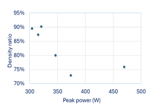
Fig .5 Printed copper density ration as a function of laser peak power
Figure 6 depicts the printed density ratio versus the spatial overlap of pulse-to-pulse, showing an optimal peak power range of 300-350W.
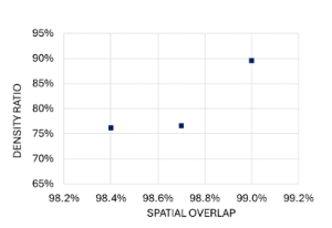
Figure 6. Printed copper density ration as a function of spatial overlap of pulse to pulse.
In this study, the highest achieved material density ratio of the printed copper was approximately 90%. This density ratio is attributed to the presence of voids within the material. The greater the number of voids, the lower the density.
To observe and analyze these voids, we cut the solid cylinder into two pieces and examined the cut cross-section using SEM. For comparison, we also cut a standard copper block and imaged its cross-section morphology. Figure 7 shows the SEM images of taken from cross-section of the printed copper (A) and standard copper (B), respectively.
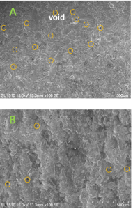
Figure 7. SEM images of the cross-section of the printed copper (A) and standard copper (B).
The SEM images clearly showcase a higher void density in laser-printed copper compared to standard copper. Our further investigation has discovered that the voids can be reduced by increasing pulse width, post-annealing, laser penning, and especially by elevating the substrate temperature during the 3D printing process. We will report our findings in a future article.
Contact: Jack Zhang, (Ph.D.)
Email: JZhang@a-optowave.com