Although ultrafast lasers have largely replaced deep-UV (<300nm) lasers in most laser micro-processing applications due to their unbeatable advantages—such as high power, high frequency, excellent light coherence, high reliability, and user-friendliness. DUV lasers remain indispensable for certain applications. These applications include surface micro-engineering, biomaterials and thermal-sensitive organic material processing, LCD/LED/LD device manufacturing, and semiconductor device fabrication. Deep-UV lasers are essential in these areas because they provide higher photo-energy necessary for chemically dissociating molecules and achieving precise processing at the desired position due to shallow penetration depth, as shown in Table 1.
| Table 1. Major applications | |
| 1. | Cutting & drilling thin biomaterials or organic materials |
| 2. | Annealing Transparent conductor (ITO) semiconductor (IGZO) film |
| 3. | Lifting semiconductor chips (GaN) off substrate |
| 4. | Patterning on Semiconductor (Si/SiO2) |
| 5. | Others |
As a competitor, deep-UV excimer lasers with wavelengths of 157 nm (F2), 193 nm (ArF), and 248 nm (KrF) still play an important role in surface processing, such as annealing, patterning, and modification, due to their unique advantages, including high-power energy, large beam size, and beam shaping capabilities. However, due to significant operational, maintenance, and beam focusing challenges, excimer lasers have been largely replaced by fiber or DPSS lasers in the field of laser micro-processing.
As an alternative to deep-UV excimer lasers, DPSS deep-UV lasers with wavelengths of 266 nm and 213 nm, resulting from the 4th and 5th harmonic generation of the fundamental 1064 nm wavelength laser, have been widely employed in micro-processing applications requiring deep-UV lasers. Additionally, ultrafast deep-UV lasers have begun to be used in industrial laser micro-processing.
AOC is a leading laser company specializing in the development and manufacturing of DPSS 266nm lasers, providing customers with industry-standard products. Figure 1 showcases the ns-266nm and ps-266nm lasers, respectively.
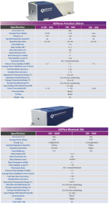
Figure 1. AOC ns-266nm and ps 266nm laser specification.
Compared to DPSS 532nm and 355nm lasers, the lower power and long-term reliability of DPSS 266nm lasers are significant limitations for large-scale processing.
Laser direct writing involves localized photochemical sintering and annealing of coated organic precursors, such as nano-ink or sol-gel. This process leverages the high photo-energy of 4.66 eV to dissociate organic molecules and the excellent focusing ability of the laser to achieve micro-sized patterning. Essentially, the annealing and sintering process converts a smooth, porous ink film into a dense, crystalline film within a precisely defined zone. This technique is particularly applied in the fabrication of advanced transparent flexible display devices. Figure 2 illustrates a schematic diagram of the laser photo-sintering and annealing process for dried ink or sol-gel coatings.
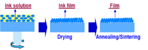
Figure 2. Schematic diagram of pulse laser heating process
Figure 3 displays the electrical conductivity of the ITO film, which has been processed using pulsed ns-266nm laser annealing on an ITO-containing Sol-Gel coating.
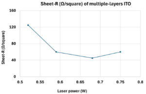
Figure 3. Electrical conductivity of the ITO film processed by AOC ns-266nm laser
Figure 4 showcase the transistor performance of the IGZO film, which has been fabricated using pulsed ns-266nm laser annealing on an In-Ga-Zn-containing Sol-Gel coating. The 266nm laser has been recognized as an ideal choice for processing solution-based transparent flexible devices.
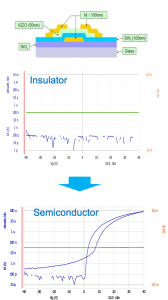
Figure 4. Semiconductor behavior of the IGZO film processed by AOC ns-266nm laser
New generation wide band-gap III-VI semiconductor (GaN) chip fabrication is divided in three steps of (i) GaN film grown by CVD on sapphire substrate because of index-matching; (ii) chip processing; (iii) chip transferring from sapphire substrate to designed device substate for further processing. Because of transparency of sapphire, using pulsed laser-forward-transfer technology can selectively transfer the individual GaN chips onto the device substrate without damaging the chips. The key parameters for controlling the process include (i) laser fluence, (ii) pulse duration and repetition rate, (iii) beam homogeneity, and (iv) thermal management. Figure 5 depicts the schematic drawing of the laser-induced forward transfer process used to deposit individual GaN chips onto the designed substrate.
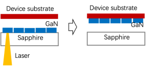
Figure 5. Schematic diagram of pulse laser lift-off process
It should be noted that both deep-UV excimer lasers and 266 nm lasers have been used for this process. As shown in Table 2, a comparison of the two laser sources is provided. While DPSS-266 nm lasers can potentially replace excimer lasers for the lift-off of GaN chips, it requires careful consideration of the factors mentioned in the table.
Table 2. Comparison of excimer laser and DPSS laser
| Laser source | Advantages | Disadvantages |
| Excimer laser (193nm, 248nm) | 1. Higher pulse energy and larger focal spot size can improve the efficiency of the lift-off process for certain applications. 2. Easy beam shaping allows for a uniform focused beam, enhancing lift-off uniformity. |
1. Lower frequency, typically in the range of 1 Hz to several hundred Hz |
| DPSS laser (266nm) |
1. More compact and robust with lower maintenance and better beam quality. 2. High frequency operation up to a few hundred kHz to achieve high throughput. |
1. Low pulse energy. 2. Difficulties in beam shaping to achieve a uniform focused beam |
Figure 6 illustrates an example of GaN chip lift-off from sapphire substrates using a 266nm laser. Recent advancements demonstrate that efficient and high-quality lift-off has been achieved with a ps-266nm laser.
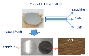
Figure 6. GaN chip lift-off from sapphire substrate
Traditionally, deep-UV lasers, such as 266nm lasers, are used for scribing semiconductor (Si, SiC) and transparent display (LCD) devices to minimize the heat-affected zone (HAZ). Recently, fs-lasers and ps-UV lasers are being considered as alternatives to deep-UV ns-lasers, especially for high-speed scribing due to their higher laser frequency. A highly effective option is the use of ultrafast deep-UV lasers like the ps-266nm laser. Figure 7 illustrates the scribing of SiO2/Si wafer using both ps-266nm and fs-515nm lasers. It clearly shows better quality using the ps-266nm laser compared to the fs-515nm laser. This is likely due to the higher penetration depth of the 515nm wavelength in Si, which generates more particles.
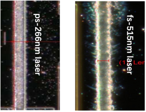
Figure 7. Scribing SiO2/Si wafer using ps-266nm laser and fs-515nm laser, respectively.
Another typical example is the use of a ns-266nm laser for scribing LCD devices. Figure 8 shows the laser scribing of a glass-based LCD wafer followed by mechanical breaking, resulting in a clean cutting edge on both the front and back surfaces.
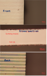
Figure 7. Scribing of LCD device using ns-266nm laser.
The main obstacle in using a ns-266nm laser for processing is its typically low power output, usually less than 3W. This limitation hinders its use in production environments. Newer laser cutting technologies employ beam-shaped picosecond 1064nm or femtosecond 1030nm lasers for stealth dicing, which overcome this power limitation.
Due to extremely tight safety regulations, only a limited range of biocompatible organic materials, such as macromolecules like PLA, can be used for interventional devices in the human body. Most polymer-based materials do not meet these stringent requirements. These biocompatible macromolecules are typically highly hydrophilic.
In one of our previous projects, we used a ns-266nm laser to fabricate a transparent biochip required for eye surgery. During process development, we also considered an fs-515nm laser as a potential candidate. Both lasers can achieve a clean cut; however, the ns-266nm laser produced a cut cross-section that retained the original transparency, which was preferred and accepted by the customer.
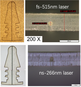
Figure 7. Cutting biocompatible macro-molecular chip.
In summary, DPSS deep-UV (266nm) lasers are employed in micro-processing only when they are essential for special device fabrication and materials processing. As a top-leading 266nm laser manufacturer, AOC will continue to provide customers with high-performance and reliable industrial products.
Contact: Jack Zhang, (Ph.D.)
Email: JZhang@a-optowave.com
AONano Precision Series DUV laser
AOPico Montauk Series DUV laser