

Laser material micro-processing technology has changed material microprocess landscape and applied in almost every major industry application from medical, aerospace, automobile, consumer electronics, photovoltaic etc. In most scenarios, laser micro-processing means a direct laser interaction with materials to generate the design features through the process such as cutting, drilling, surface structuring, surface stripping etc. The essence of laser interaction with matter is breaking chemical bonds to generate new chemical format, which could be unstable to chemicals. As a result, chemical processing can succeed in completing the material processing and device fabrication. Thus, by using laser energy to activate or accelerate chemical reactions, this technique enables highly localized processing, minimizing thermal damage to surrounding area, where this precision, cleanliness, and material integrity are critical when working with complex materials, composites, or sensitive structures.
Table 1 lists three common types of laser-assisted chemical processing, each playing a significant role in industrial device fabrication
| 1. Laser-Induced Plasma Etching (LIPE) | This process is widely used for etching semiconductor materials like silicon. Using a laser to create localized plasma accelerates chemical reactions, etching material in a highly controlled and precise ways. It’s crucial for fabricating intricate microelectronic components like microchips, where precise material removal at a small scale is required. |
| 2. Laser-Activated Surface Functionalization | Lasers are used to initiate surface chemical reactions to modify a material’s properties. This process is vital in creating biocompatible surfaces on medical devices or creating specialized coatings in aerospace components, where the material’s surface properties are key to performance. |
| 3. Laser-Induced Wet Etching | This process allows for the selective removal of material by activating chemical reactions at the laser’s focal point. It’s commonly used in optical components or microfluidic devices, where fine structures must be created in glass substrates. |
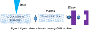


In this article, we highlight AOC’s efforts in developing laser-induced wet etching (LIWE) processes for diverse applications.
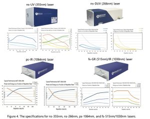
Depending on the device’s intended functionality, glass processing can be conducted either on the surface, as in the case of micro-lens arrays, or internally, as with micro-channels. For surface processing, UV (355nm) and DUV (266nm) lasers are commonly used, while internal processing typically employs picosecond (ps) or femtosecond (fs) lasers for precision.
AOC provides the industry with reliable UV (355nm), DUV (266nm), ps (532nm/1064nm), and fs (515nm/1030nm) laser options. Figure 4 details the specifications for ns-355nm, ns-266nm, ps-1064nm, and fs-515nm/1030nm lasers.

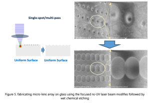
We are pleased to introduce AOC’s exploration of glass surface patterning using the Laser-Induced Wet Etching (LIWE) method. By shaping the laser beam profile, we can achieve etched surface features precisely tailored to design specifications, with etching depth directly proportional to beam intensity—higher beam density yields deeper etching. Given glass’s high optical transparency in the near-IR to visible range, utilizing UV or DUV lasers allows for precise depth control due to limited absorption, making it ideal for applications requiring exacting etch depths.
Figure 5 illustrates the fabrication of a micro-lens array using a focused ns-UV laser beam to modify the glass surface with a single shot per position, followed by chemical etching with an HF-based solution. Key processing parameters include laser fluence and etching time. This result demonstrates basic feasibility; however, actual micro-lens processing would require more complex engineering efforts.

Glass-based microfluidic devices are highly valued for applications that require durability, chemical inertness, and optical properties. They are becoming increasingly advanced with new fabrication methods, enabling even more complex functionalities in compact forms. Ultrafast laser as emerge technology has been proven to be an idea method because of multi-photon absorption. There are two approaches. One is using the tightly focused laser beam inside glass to directly remove glass material in flowing liquid and to generate micro-channels. The other one is using the tightly focused laser beam inside glass to modify glass then followed by chemical etching to generate micro-channels, as introduced in this article.
Figure 6 illustrates high aspect-ratio channels in fused silica glass created using the LIWE method. The channel width is influenced by the concentration of the etchant solution and the duration of the etching process.
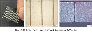
Figure 7 shows a simple microfluidic device fabricated in fused silica glass using the LIWE method. Unlike straight channel processing, 3D channel fabrication requires specific techniques to ensure uniformity across all directions.

In summary, laser-assisted chemical processing (LACP) has proven effective for specific types of device fabrication by leveraging the laser as an ‘ignitor’ and chemical solutions as an ‘etchant.’ However, due to increasing regulations on the use of toxic chemicals, LACP applications are likely to be restricted to cases where they are essential.
Contact: Jack Zhang (Ph. D).
Email: jzhang@a-optowave.com