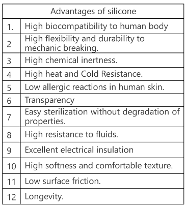
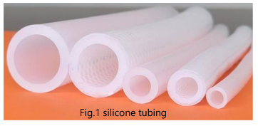
Thanks to its exceptional material properties, particularly its versatility and compatibility with the human body, silicone has found extensive use in the medical field for critical applications such as breast implants, catheters, would dressings, medical tubing, and more (see Fig. 1). Table 1 highlights the key advantages of silicone materials.
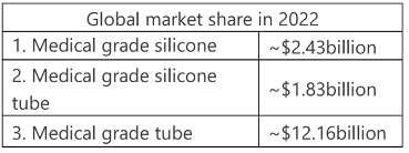
Among these medical applications, medical-grade silicone tubes play a significant role. For instance, the market size ratio of medical-grade silicone to overall silicone is approximately 74%. Furthermore, when considering the market size ratio of medical-grade silicone to all medical-grade tubes, it stands at approximately 14.8%, as indicated in Table 2.
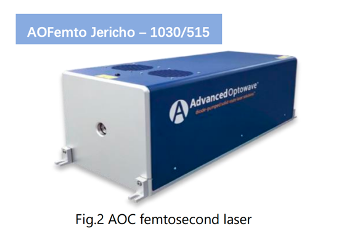
Due to its exceptional softness, traditional contact processing methods such as mechanical cutting and drilling tools require sharpness and speed to achieve clean cuts while minimizing material melting. This poses a significant challenge for mechanical tools. In contrast, laser processing offers a non-contact approach that is relatively insensitive to material softness, as long as photon energy is directed into the molecular network. This constitutes a key reason why lasers are widely employed in silicone processing tasks such as cutting, drilling, marking, and surface modification. In particular, the industrialization of femtosecond laser technology (with pulses lasting less than 10^-12 seconds) has made it possible to achieve flawless silicone processing with high quality and efficiency (see Fig. 2). Within this volume, you will find Advanced Optowave’s latest advancements in laser marking, cutting, and drilling of silicone, showcasing the cutting-edge developments in this field.
The process of marking has become essential for registering information on materials and devices, such as manufacturing dates, models, types, and barcodes. When compared to traditional printing and stamping methods that use color inks, laser direct marking offers a cleaner and more environmentally friendly labeling process. This is particularly crucial for medical devices, where avoiding external contamination is paramount.
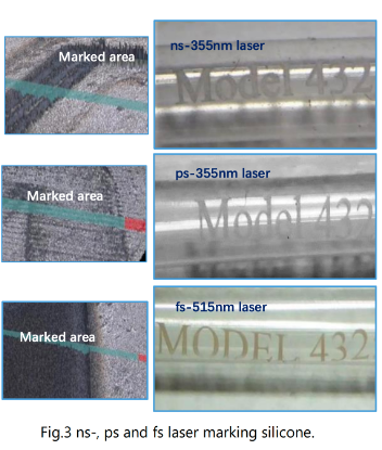
In contrast to other polymers with higher carbon content that exhibit a clear black-and-white contrast when subjected to laser marking, silicone laser marking relies on a unique approach involving light scattering and trapping through laser-generated microstructures. Consequently, only specific laser sources, such as UV-lasers or ultrafast-lasers, are suitable for marking silicone materials.
Fig. 3a-c illustrates silicone marking, using various laser sources, including ns-355nm, ps-355nm, and fs-515nm lasers, each offering distinct advantages due to their shorter pulse widths and superior contrast. An analysis of surfaces morphology using a 3D confocal microscope clearly demonstrates that fs-lasers or ps-lasers produce uniform microstructures without significant debris. In contrast, ns-UV laser result in a rougher surface with noticeable heat-affected zones (HAZ).
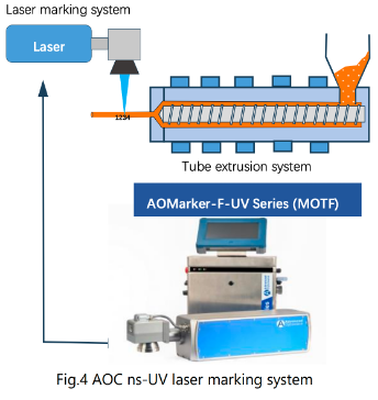
Silicone tube marking is typically employed for registering tubes immediately after the extrusion process. To effectively keep pace with extrusion, the laser marking speed needs to be swift, approximately matching the extrusion rate of around 10 feet per minute, a technique commonly known as “marking-on-the-fly” or MOTF (see Fig. 4).
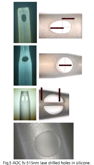
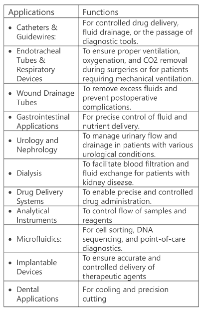
Drilling holes in silicones tubing exhibits important applications as medical device as shown in table below
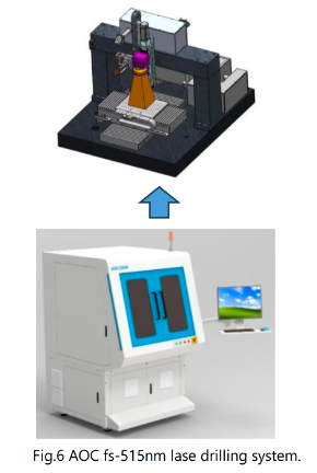
The advantages of employing femtosecond laser drilling for medical-grade silicone tubing lie in its ability to craft exceptionally precise perforations while minimizing thermal damage and lowering the risk of contamination. By employing the advanced Advanced Optowave-developed femtosecond laser micro-processing system (refer to Fig. 5), we can reliably create flawless perforations, thus ensuring compliance with device qualification standards (refer to Fig. 6).