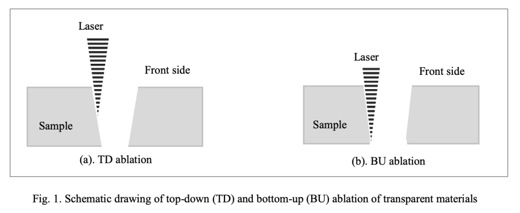
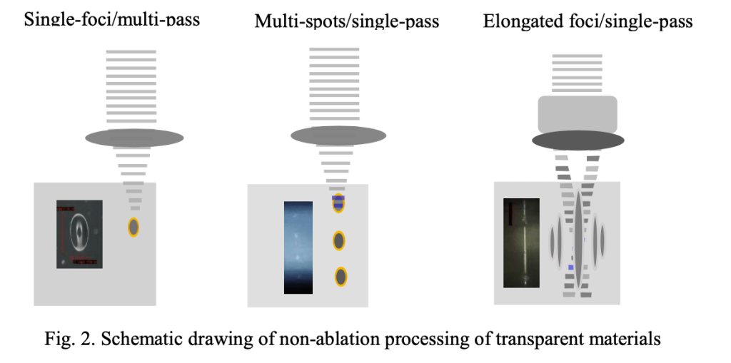
In this paper, the micro-processing of glass, sapphire, and polymers using industrial-grade nanosecond (ns), picosecond (ps), and femtosecond (fs) lasers was reported. Square/round inner contour were fabricated in glass and sapphire (0.3 to 1.1 mm in thickness) by the ablation-based cutting method using the ns, ps and fs lasers. The chipping sizes were 20 –50um with 532nm ns laser, < 10 with 1064nm ps laser, and < 5 μm with 515nm fs laser, respectively. When processed using the 532nm ns laser, the laser fluence is 5 – 10 times higher than that used in the ultrafast lasers. Outline-dicing of glass, and sapphire was conducted using a 1064 nm ps laser followed by thermal/mechanical breaking. The laser beam was shaped to form a long focal depth. Clean edges and cross-sections were observed on the processed transparent materials. Melting-free cutting of PI, and PLLA was successfully realized using a 515nm fs laser to fabricate printable electronic and medical devices. The impact of the key parameters, including pulse energy, repetition rate, focal spot size, beam shaping was systematically studied. The best ablation efficiencies of glass and sapphire obtained were 0.3 – 0.4mm3/(W•min.) when using the ultrafast lasers, which is much lower than that of polymers (2.0 – 4.0mm3/(W.min).).

